It is not so easy but I want very much to give a try.
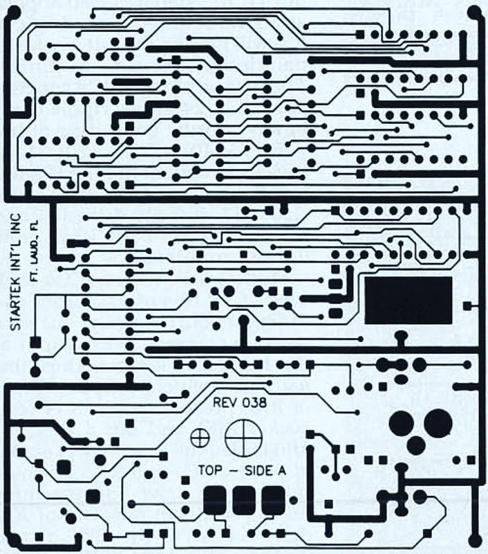
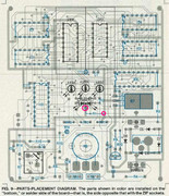
Here are the pcb prints that I take from the magazine:
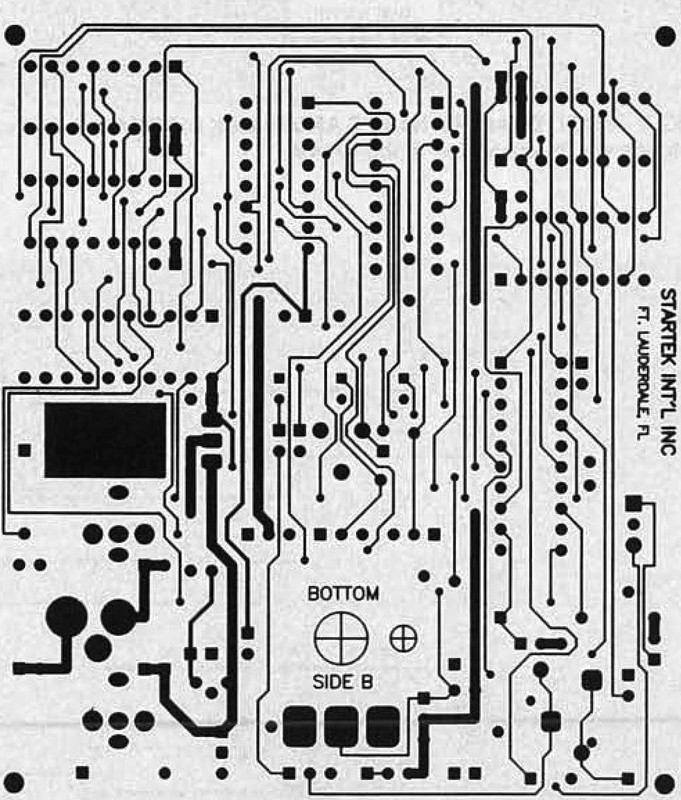
And here is the pcb mask:

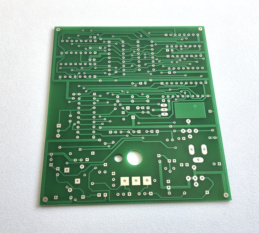
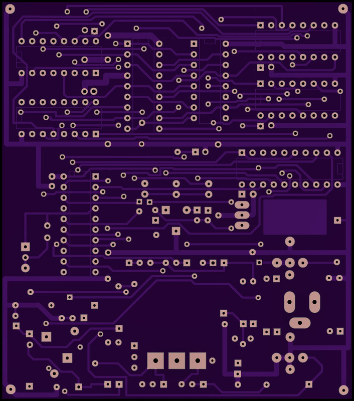
Here is my work so far:

Any suggestions are more than welcome.
Thanks.

That's not a problem, since they are easy to do at home (photo-hatching process), for a single sided, board.Muttley Black wrote: ↑Tue May 12, 2020 9:19 pm Hello RMartins.
First i have to say that i am not well experience making pcb's. I do every project first for my own pleasure and practise.
Well, it shouldn't be hard, and there are several tutorials around for it.Muttley Black wrote: ↑Tue May 12, 2020 9:19 pm The part list yes, It is available (look at the end of this post). About the square footprint that have to be at the pin 1 and only, i mess it around accidentally. It is an easy fix don't worry about that. I try the mimicking by hand method cause i wont the final result to be almost as the original. Trying that by create the schematic first on kicad and then rooting the pcb is hard for me.
Here is the magazine on pdf.
https://www.dropbox.com/s/m1yeyfrn30gsh ... 1.pdf?dl=0
If you look at the schematic in the magazine, page 37, you will see that in fact the double led kathode, is connected to ground through R1.Muttley Black wrote: ↑Wed May 13, 2020 10:26 pm ... If you look at the pcb mask, the one that have the components layout, LED4 (green/red) with the 3 legs sawing the negative leg soldered in the ground (top side), but in bottom side of the board soldered again in a ground track ( bottom side) but that time through R1 resistor (91ohm) for current limitation. How that led have current limitation in neg leg if already its soldered in clear ground on top side? Or the pcb prints have errors, or i didn't understand that part well.
...
Assuming the board does NOT have DIP components mounted on both sides, you still have some DIP square pins on the wrong position, that are not in pin 1 position, since they appear on one side of the chips but in some other locations they appear on the other side of the chips. If components are all on the same side (which is usually the case), the pin 1, must be always on the same side of the chip.

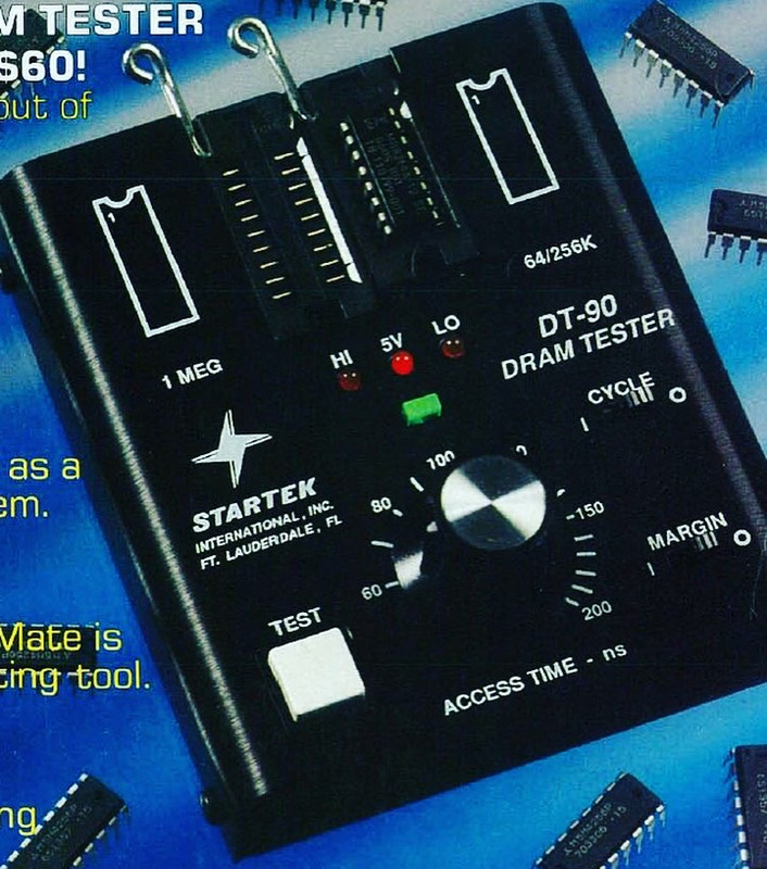
Well... i receive an email today.From my research, the only person i know who has one Startek DT-90, is one guy from the USA who repairs arcade machines. Is the same guy if i am not mistaken who buy's the last stock from the Startek company. Before some years sold the last one but kept one from himself.
I have send him the emails for some photos or info's but never get an answer. Some people don't wont to help...