New open lower RAM module design (photoessay)

For experts to discuss very technical stuff and newbies to ask why the Spectrum they bought off ebay doesn't work.
dfzx
Manic Miner
Posts: 681
Joined: Mon Nov 13, 2017 6:55 pm
Location: New Forest, UK
Contact:

New open lower RAM module design (photoessay)

Post by dfzx »

Last summer I found myself with a couple of 48Ks with dead lower memory. I was therefore in the market for the modern lower memory boards which are a standard solution to this problem. As I investigated I was surprised to find that there doesn't appear to be an open design for these boards. Retroleum sell one but it's not an open design; there's one detailed at zigg.net but that's no longer available and was never an open design as far as I can tell; this chap tried to create one but doesn't seem to have got it working. I thought I'd have a go myself.

Just the one slight problem: I didn't know anything about digital electronics or circuit design. So I spoke with some clever people, watched an awful lot of YT videos and learned a bit about it. Eventually I managed to create a credible looking circuit which I needed to get made into a PCB. Another slight problem: I didn't know anything about PCB design or layout or fabrication either. I learned more and late last summer a pack of little green circuit boards dropped on the doormat. I needed to learn a bit about soldering surface mount components, and lamented I didn't try this before I got old and my eyesight stopped working properly, but I got there:

Image

At first glance it looked like it worked, but actually it didn't. The Z80 was happy, but if you look at the screen you can see little artefacts in the display. These constantly flicker around. I termed them "sparkles." They were worst when the Spectrum was just started up; after about 20 minutes they pretty much disappeared. Odd.

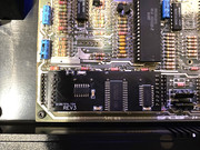
After a lot of reviewing of my circuit and the datasheets of the components I was using I concluded that the problem was that the modern SRAM IC I was using wasn't holding the data on its output bus long enough for the ULA to come and fetch it. The Z80 was OK, but the ULA is a fussier thing. Someone cleverer than me suggested delaying the board's input CAS signal to slow things down just a tad. In classic ZX fashion I lashed up my very own cockroach type thing:

Image

This seemed to solve the problem:

Image

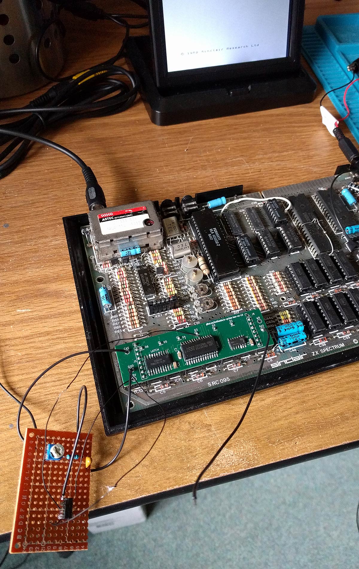
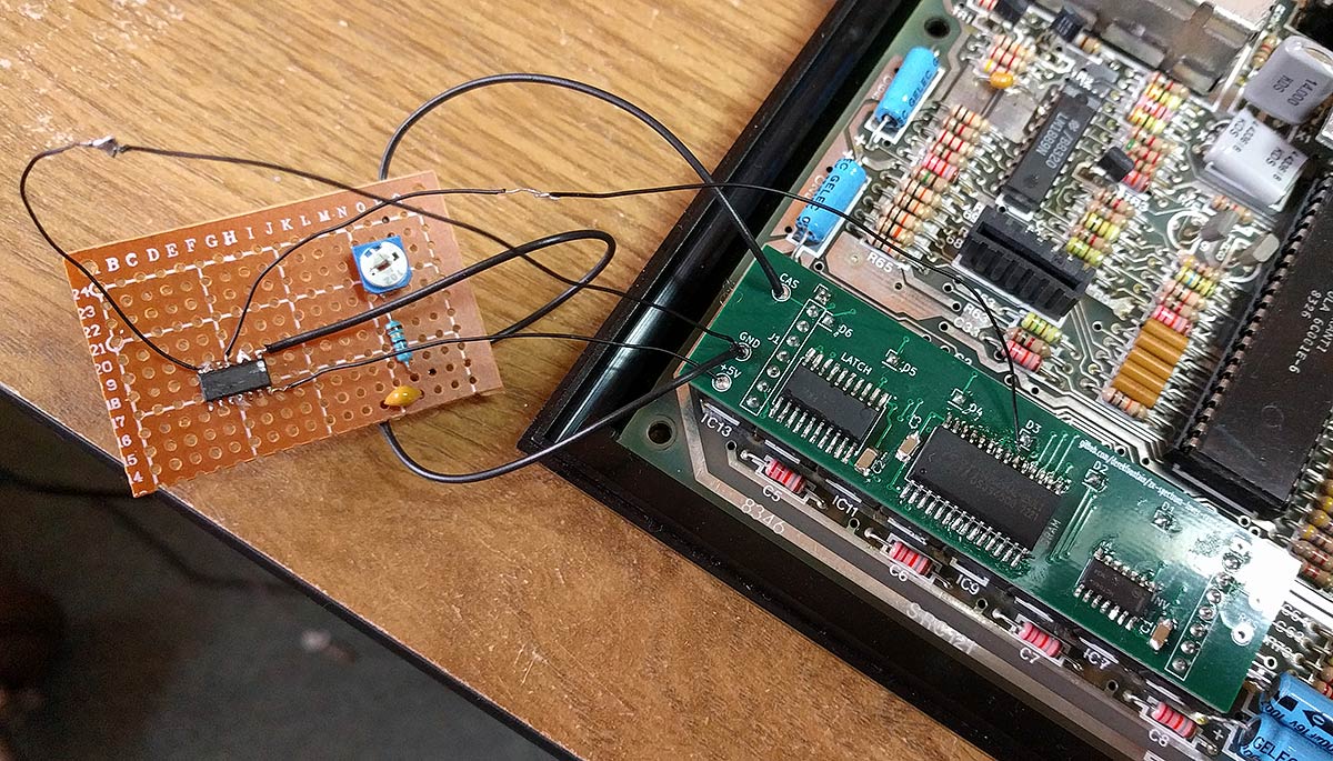
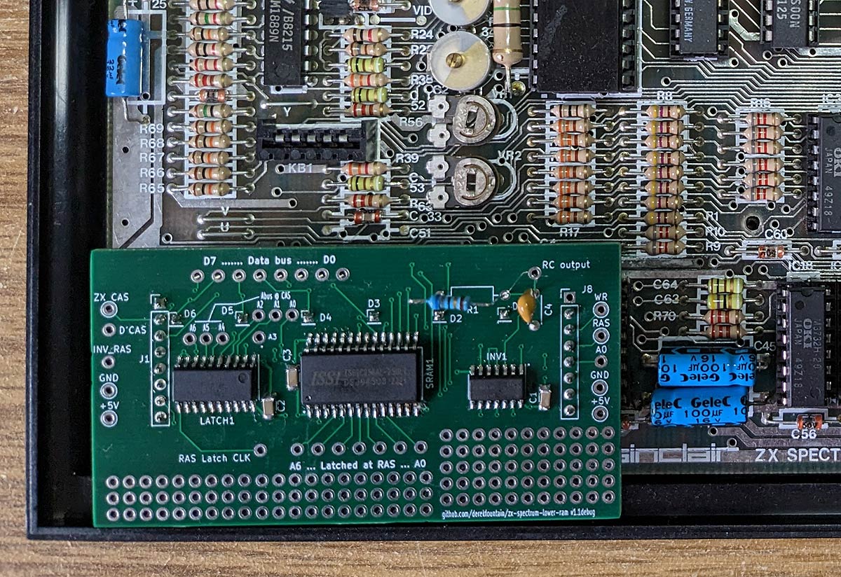
It was time to get v1.1 fabricated. Something else I'd learned was that it's not easy to attach oscilloscope probes to SMD components, so for this version I created a "breakout" board which gave access to test points:

Image

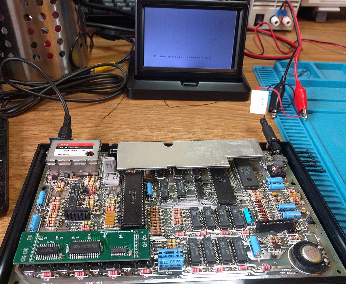
This one worked, and it worked better than v1.0 with the cockroach. "Better grounding and signal integrity" I was advised. I made up a non-breakout version and with just one little bodge it was looking good:

Image

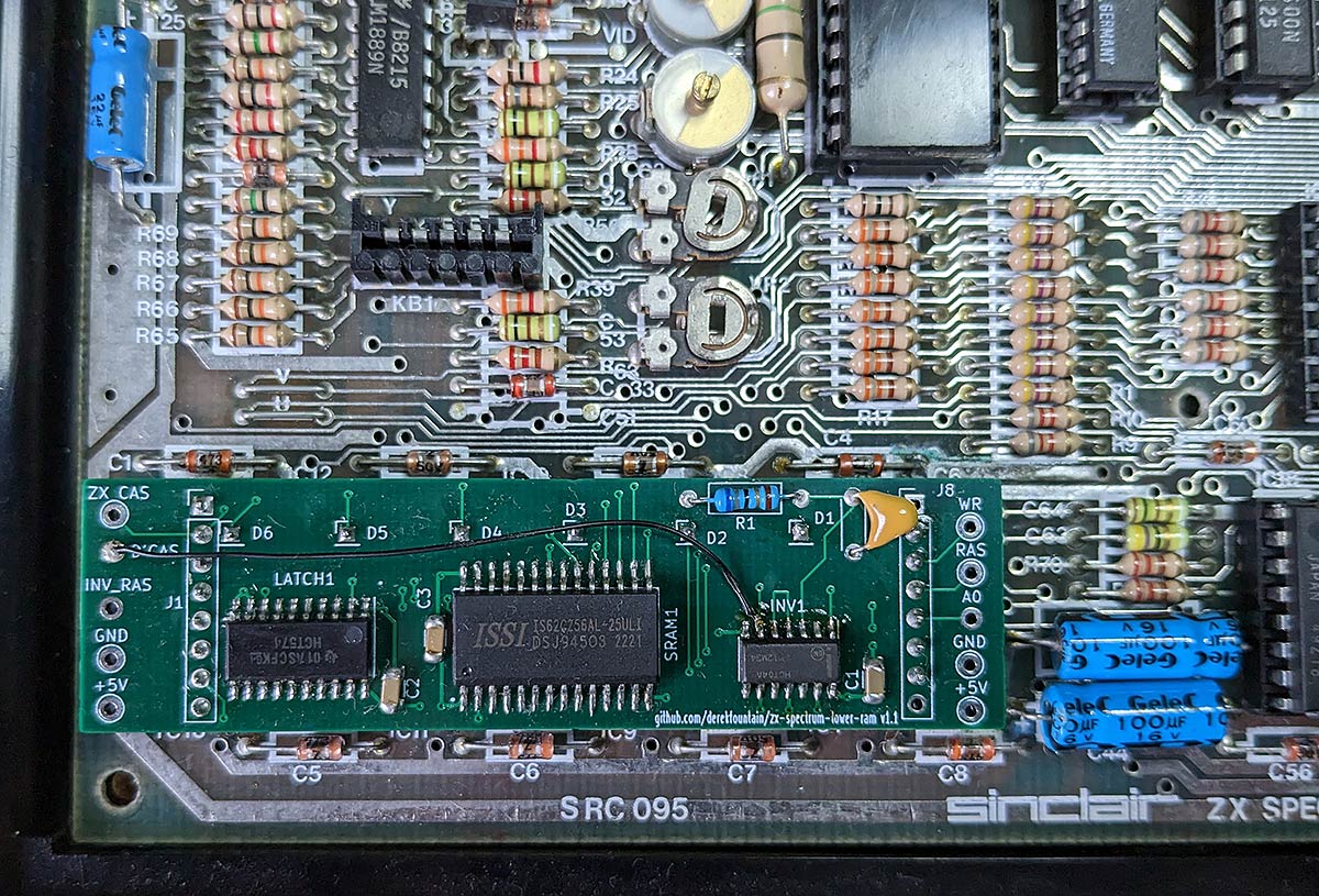
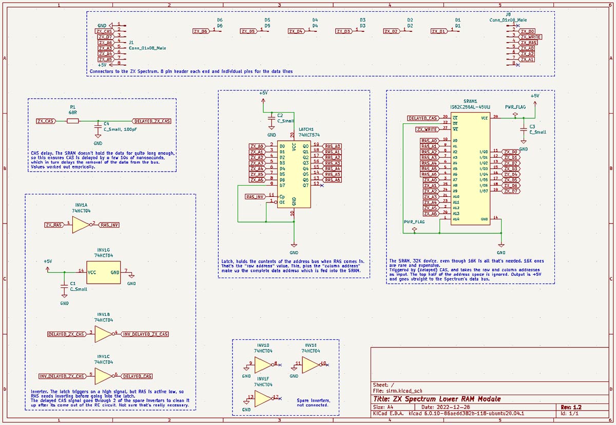
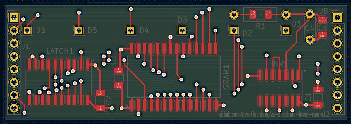
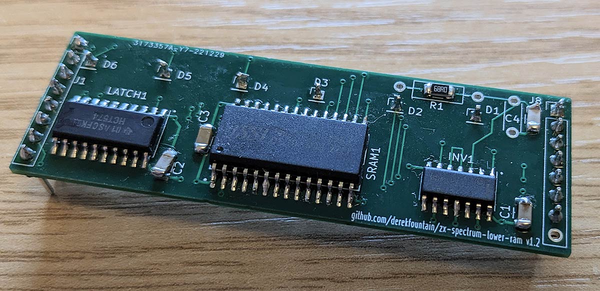
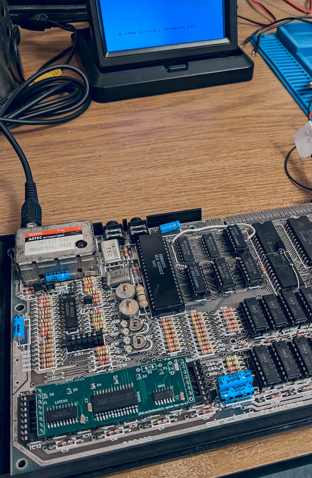
Version 1.2 went off for fabrication. This one lost all the test points and was created on a 1.00mm thick board, as I was becoming conscious that I was going to have to get the Spectrum's keyboard back on at some point. The final circuit and layout looks like:

Image

Image

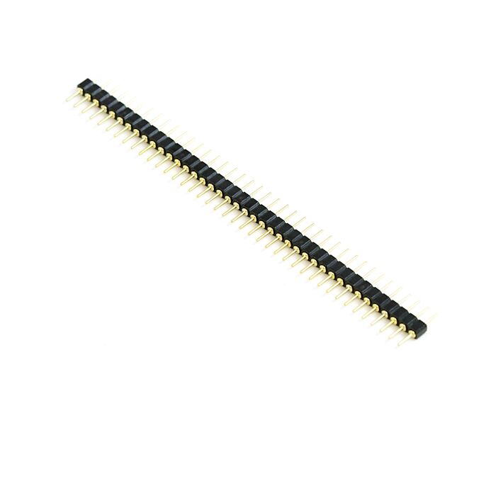
When the boards arrived I made one up and it worked! There then opened another rabbit hole, which was the mechanical challenge of getting the board to fit under the Spectrum's keyboard. I'd used Arduino-style 11mm header pins:

Image

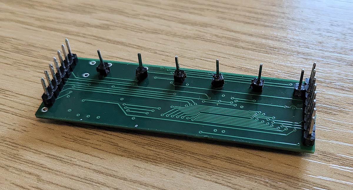
which worked, but made it sit far too high:

Image

I went back to one of my earlier attempts to see how easy it was to clip the headers to length. Not easy, it turns out. Those headers are really hard so big cutters are required for them, and big cutters tend to mangle the ends of the pins.

Image

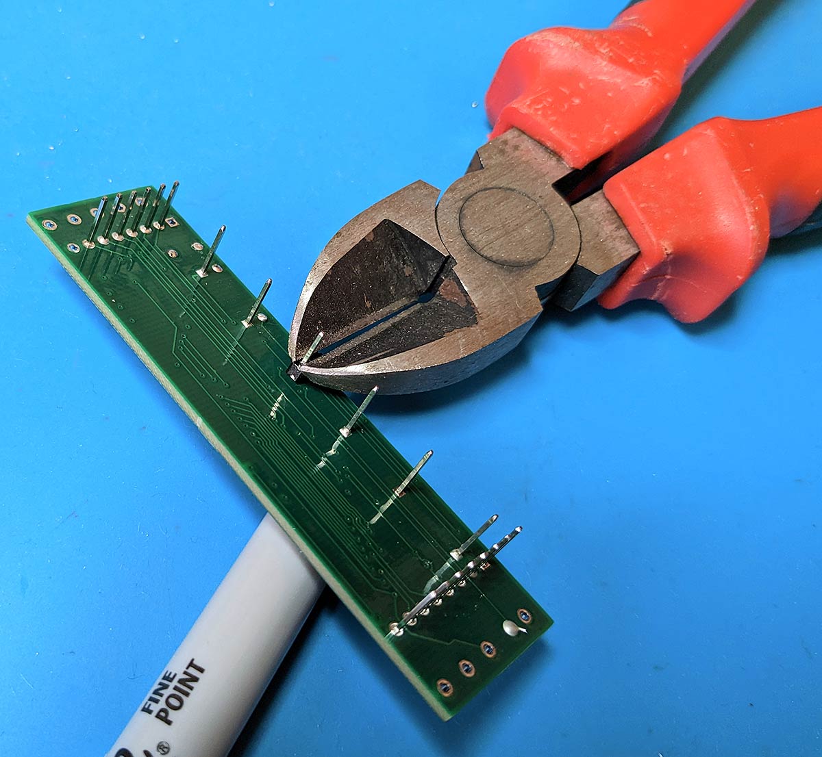
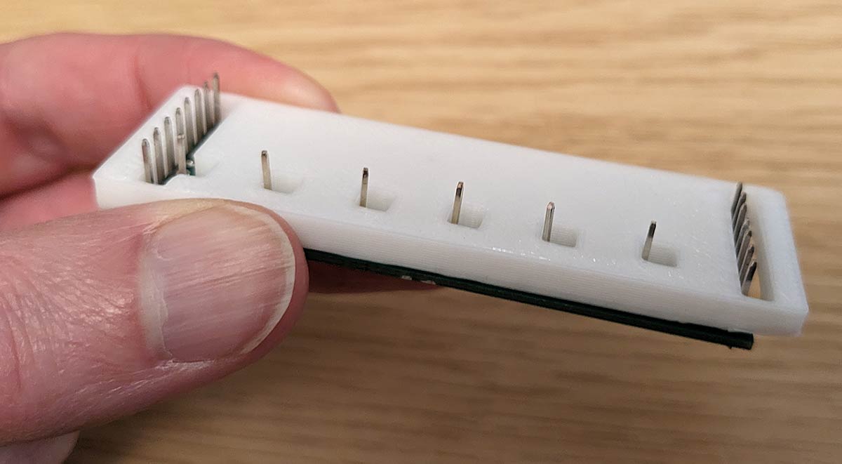
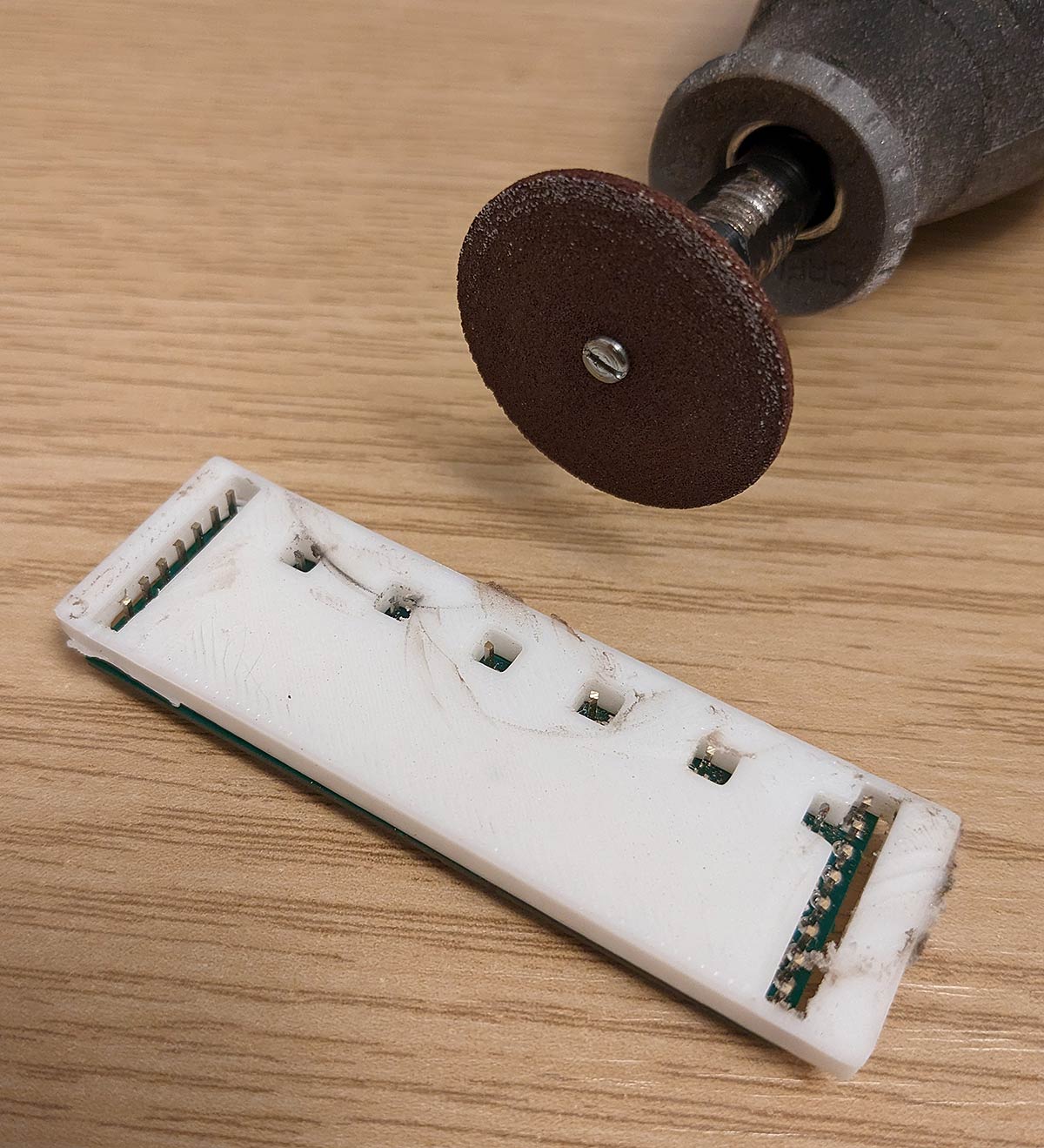
Plan B was to grind the pins down with a Dremel, but that didn't work too well either. The pins all need to be the right length to fit in the sockets; get one too long and the board stands too proud, get one too short and that pin doesn't make contact and the board is ruined. I needed them all to be 4.0mm. The only option, I decided, was to make a jig on the 3D printer to guide the Dremel:

Image

That allowed me to grind down the pins with the precision required:

Image

The result was as required:

Image

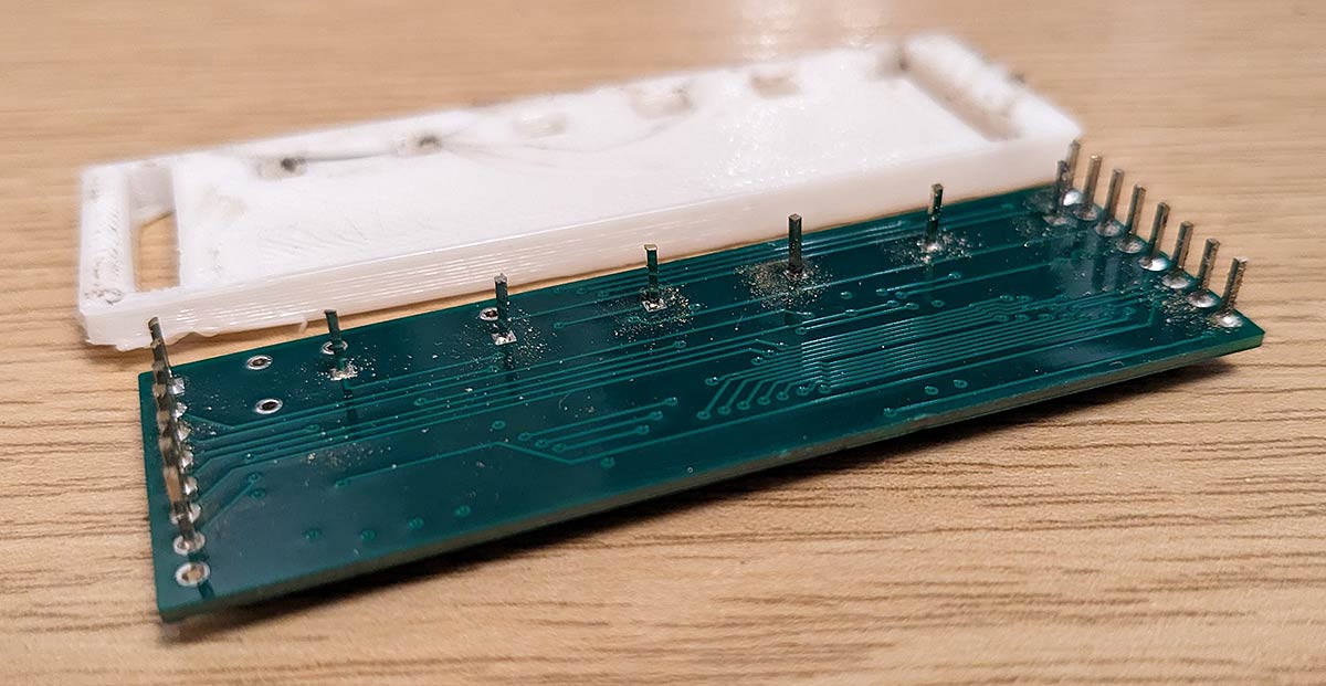
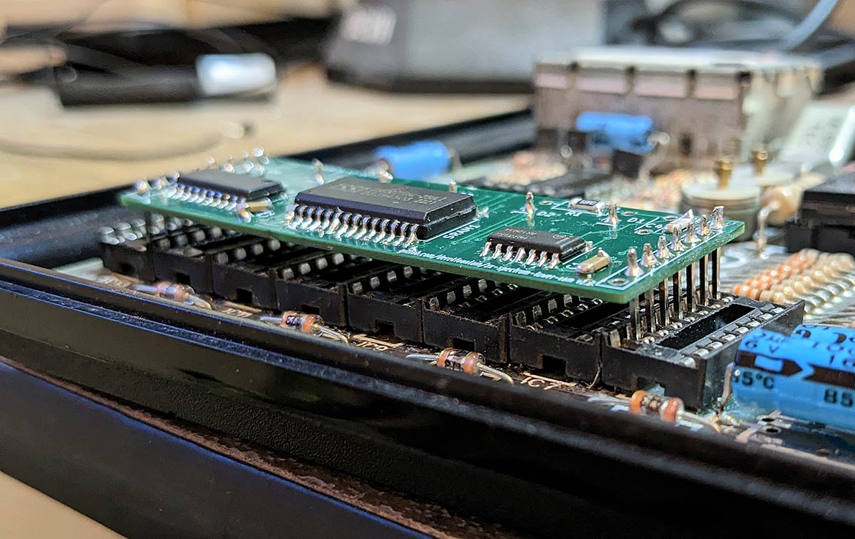
which leaves the final board ready to use:

Image

It just presses into the sockets:

Image

and the keyboard fits over the top:

Image

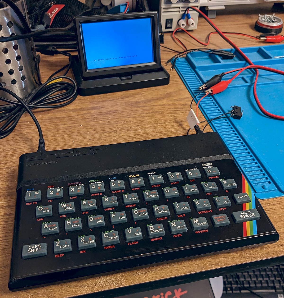
Success! And it only took a few months and vast amounts of work to create something you can buy from Retroleum for £13!

The project, its design and source files, together with build instructions and the files for 3D printing the jig are all available on my Github page. A few more technical details about how it works are on my website.
Derek Fountain, author of the ZX Spectrum C Programmer's Getting Started Guide and various open source games, hardware and other projects, including an IF1 and ZX Microdrive emulator.
hatman72
Drutt
Posts: 19
Joined: Mon Sep 13, 2021 4:15 pm

Re: New open lower RAM module design (photoessay)

Post by hatman72 »

Brilliant! I really enjoyed reading about that and the way that you have worked through it, especially given your lack of prior experience.
worcestersource
Manic Miner
Posts: 524
Joined: Thu Feb 03, 2022 11:05 pm

Re: New open lower RAM module design (photoessay)

Post by worcestersource »

Excellent work. I love stories like this!
User avatar
flatduckrecords
Manic Miner
Posts: 785
Joined: Thu May 07, 2020 11:47 am
Location: Oban, Scotland
Contact:

Re: New open lower RAM module design (photoessay)

Post by flatduckrecords »

Wonderful! Thanks for sharing the story, and thank you for open-sourcing your work. ❤️

(P.s. Your comment about the “sparkles” is really interesting, I’m sure I’ve observed that on one of my repaired Spectrums. I’ll take a closer look with that in mind, thanks for the tip!)
cj7hawk
Manic Miner
Posts: 361
Joined: Sat Sep 25, 2021 9:11 am

Re: New open lower RAM module design (photoessay)

Post by cj7hawk »

Fantastic Work ! It's great that you completed it -

You can get smaller "machined" pins also which may save the dremel step that you undertook - they are about the same price as pins, and have a long side and a short side and are used to turn "PCBs" into "Chips" and the like.

Google Breakaway Machined Pin Headers to find some local ones - They look like this.

Image

Looking forward to seeing your next project :)

David
zx64
Manic Miner
Posts: 211
Joined: Sat Jul 11, 2020 3:25 am
Location: Australia

Re: New open lower RAM module design (photoessay)

Post by zx64 »

Nice work.

You could cut the other end of the pin (after soldering, with cutters). The one on top of pcb. You know you can slide the black plastic up and down on the pins, do you? So, insert pins into ram sockets, adjust the height on the plastic, place your pcb on top, solder, cut off excess pins.
zx64
Manic Miner
Posts: 211
Joined: Sat Jul 11, 2020 3:25 am
Location: Australia

Re: New open lower RAM module design (photoessay)

Post by zx64 »

How much did you need to delay CAS? As an alternative to the capacitor you could try to use 2x spare inverters you have
dfzx
Manic Miner
Posts: 681
Joined: Mon Nov 13, 2017 6:55 pm
Location: New Forest, UK
Contact:

Re: New open lower RAM module design (photoessay)

Post by dfzx »

zx64 wrote: Wed Jan 18, 2023 12:47 am You could cut the other end of the pin (after soldering, with cutters). The one on top of pcb. You know you can slide the black plastic up and down on the pins, do you? So, insert pins into ram sockets, adjust the height on the plastic, place your pcb on top, solder, cut off excess pins.
Argh! How did that not occur to me? :o

It's all a learning exercise, and I'm embarrassingly green, but honestly, I should have spotted that. :lol:
Derek Fountain, author of the ZX Spectrum C Programmer's Getting Started Guide and various open source games, hardware and other projects, including an IF1 and ZX Microdrive emulator.
dfzx
Manic Miner
Posts: 681
Joined: Mon Nov 13, 2017 6:55 pm
Location: New Forest, UK
Contact:

Re: New open lower RAM module design (photoessay)

Post by dfzx »

cj7hawk wrote: Wed Jan 18, 2023 12:12 am Google Breakaway Machined Pin Headers to find some local ones
Cuh, I spent hours, literally hours, poring over lists of header pins trying to find those! I knew something like that must exist because I've seen them on devices I've purchased. Stuffed if I could find them though. Oh well, something else learned, thanks! :geek:
Derek Fountain, author of the ZX Spectrum C Programmer's Getting Started Guide and various open source games, hardware and other projects, including an IF1 and ZX Microdrive emulator.
dfzx
Manic Miner
Posts: 681
Joined: Mon Nov 13, 2017 6:55 pm
Location: New Forest, UK
Contact:

Re: New open lower RAM module design (photoessay)

Post by dfzx »

zx64 wrote: Wed Jan 18, 2023 12:56 am How much did you need to delay CAS?
I ended up with a 100pF capacitor and a 68ohm resistor, so the time constant is about 7ns. The signal then goes through 2 of the inverters to clean it up before it goes into the SRAM as the trigger. The HCT family inverter I used has a propagation time of 15ns to 20ns depending on temperature. So at room temperature the CAS delay is about 40ns.
zx64 wrote: Wed Jan 18, 2023 12:56 am As an alternative to the capacitor you could try to use 2x spare inverters you have
To be honest I didn't really know what I was doing and I worked it out empirically. The "cockroach" I made was the CAS RC delay circuit and it had a variable resistor which allowed me to tune the delay. I just watched the screen, fiddled with the variable resistor, and when the sparkles went away I measured the resistance of the variable resistor and declared that that, plus the 100pF capacitor I happened to choose, defined the delay I required.

I don't think this is quite how you're supposed to do digital electronics. :lol:
Derek Fountain, author of the ZX Spectrum C Programmer's Getting Started Guide and various open source games, hardware and other projects, including an IF1 and ZX Microdrive emulator.
zx64
Manic Miner
Posts: 211
Joined: Sat Jul 11, 2020 3:25 am
Location: Australia

Re: New open lower RAM module design (photoessay)

Post by zx64 »

dfzx wrote: Wed Jan 18, 2023 11:16 am I don't think this is quite how you're supposed to do digital electronics. :lol:
But it's doe all the time :D
Spectrum itself has it, to delay CAS for the upper memory.
In the right bottom corner on schematics
https://spectrumforeveryone.com/wp-cont ... matics.gif
Image
dfzx
Manic Miner
Posts: 681
Joined: Mon Nov 13, 2017 6:55 pm
Location: New Forest, UK
Contact:

Re: New open lower RAM module design (photoessay)

Post by dfzx »

zx64 wrote: Tue Jan 24, 2023 3:33 am Spectrum itself has it, to delay CAS for the upper memory.
Yes, I'm starting to realise this. :) I've got the ULA book now, and there's quite a bit of discussion in there about how inverters were used to slow down signals until something started working.

As a professional software engineer this is complete anathema to me. The idea of "just throwing a sleep(1); in there" to bypass a race condition is common among inexperienced software developers, but us greybeards know that horrible hacks like that just lead to technical debt.

In the hardware world it seems different. "If the timing works today it'll work tomorrow because in hardware nothing changes." And indeed, my memory board has been working for weeks now. So it must be good. :)
Derek Fountain, author of the ZX Spectrum C Programmer's Getting Started Guide and various open source games, hardware and other projects, including an IF1 and ZX Microdrive emulator.
AndyC
Dynamite Dan
Posts: 1406
Joined: Mon Nov 13, 2017 5:12 am

Re: New open lower RAM module design (photoessay)

Post by AndyC »

One of my favourite stories from Amstrad's take over from Sinclair was the engineers, who had been meticulous in designing the CPC464 etc, looking at the Spectrum PCB and being horrified at how hacked together it was and baffled by how it worked at all... :lol:
cj7hawk
Manic Miner
Posts: 361
Joined: Sat Sep 25, 2021 9:11 am

Re: New open lower RAM module design (photoessay)

Post by cj7hawk »

dfzx wrote: Wed Jan 18, 2023 9:52 am Cuh, I spent hours, literally hours, poring over lists of header pins trying to find those! I knew something like that must exist because I've seen them on devices I've purchased. Stuffed if I could find them though. Oh well, something else learned, thanks! :geek:
I feel your pain. Same thing happens to me all the time... Sometimes I just google weird stuff barely related to what I want hoping I'll get some hits... It was easier back in the day when there was less choice and the Radio Spares ( or whatever the UK equivalent was ) "picture book" let us choose stuff that looked right rather than having to google it.

Recently I wanted some 40 pin plugs in the shape of a z80 that connect to an IDC cable... Took me a while to find some, and all were about $80 or so, but after a few searches, I found the right terminology... Half an hour later ( maybe an hour? ) I finally found the right part on a local supplier for about $5 each.
drdivago
Dizzy
Posts: 57
Joined: Sat Apr 02, 2022 3:11 pm
Location: Barcelona, Spain

Re: New open lower RAM module design (photoessay)

Post by drdivago »

Hi,

When I upload the Gerber files (fab1.2.zip) to JLCPCB the system tells me that it's a 4-layer circuit: is that correct? :?:

Thanks

Ciao
Leo
dfzx
Manic Miner
Posts: 681
Joined: Mon Nov 13, 2017 6:55 pm
Location: New Forest, UK
Contact:

Re: New open lower RAM module design (photoessay)

Post by dfzx »

drdivago wrote: Wed Jan 25, 2023 2:30 pm When I upload the Gerber files (fab1.2.zip) to JLCPCB the system tells me that it's a 4-layer circuit: is that correct? :?:
It is indeed, yes. I needed separate power and ground planes.
Derek Fountain, author of the ZX Spectrum C Programmer's Getting Started Guide and various open source games, hardware and other projects, including an IF1 and ZX Microdrive emulator.
drdivago
Dizzy
Posts: 57
Joined: Sat Apr 02, 2022 3:11 pm
Location: Barcelona, Spain

Re: New open lower RAM module design (photoessay)

Post by drdivago »

dfzx wrote: Wed Jan 25, 2023 2:43 pm It is indeed, yes. I needed separate power and ground planes.
Great, thanks for the quick confirmation!
mark8bit
Dizzy
Posts: 59
Joined: Mon Sep 13, 2021 6:18 pm

Re: New open lower RAM module design (photoessay)

Post by mark8bit »

nice project,, i was looking into this and found this post, i used some of your ideas but made a 2 layer pcb.. i jumbled up the address & data lines in order for minimize the journey the traces had to make. Couldn't get it to work on the breadboard but ordered boards anyway not being overly optimistic that i hadn't made mistakes arrived today from china and soldered it up and it works great.. need to test further but it passes all the diag tests..

https://photos.app.goo.gl/B48egVM2W6Q2xVzNA
dfzx
Manic Miner
Posts: 681
Joined: Mon Nov 13, 2017 6:55 pm
Location: New Forest, UK
Contact:

Re: New open lower RAM module design (photoessay)

Post by dfzx »

Interesting, you've done a complete new layout. You've made it quite a bit bigger, spanning the whole of the DRAM array by the look of it. (Mine spans only to the inner sides of the outer most ICs.) What mounting pins did you use? I didn't have a clue what I was doing with those. :)

I think if I were doing it again I'd probably go 2 layer. I used the extra layers for ground and VCC planes, which, as you've demonstrated, isn't really necessary. It did make life easier when I was trying to get it working though.

Will you be opening your design for others to use?
Derek Fountain, author of the ZX Spectrum C Programmer's Getting Started Guide and various open source games, hardware and other projects, including an IF1 and ZX Microdrive emulator.
mark8bit
Dizzy
Posts: 59
Joined: Mon Sep 13, 2021 6:18 pm

Re: New open lower RAM module design (photoessay)

Post by mark8bit »

ive added some more pics to the shared folder,,
schematic + board pics
i am always happy to share if anybody is interested.. i was looking at github but dont really understand it, i will look some more ..
my original plan was to use through hole only components but with the size of them that wasn't going to work as i have some 128k Sram 32 pin that i was going to try that i brought for another project that has yet to be done..
** the plan was to bit bang a SD card from the I/O of the spectrum then load a game/snapshot into the Sram in 16 kb junks and load the SRam into the ROM space and copy to the ram then repeat with the next 16kb etc **
but that's another story, I have loads of spectrum projects that are in flux
i may make a another revision of the lower ram and slim it down a bit, it took me ages to run all the traces in easy EDA, i also did a version the same but using the auto trace but have not tried that one yet.

at the moment i have used standard header pins (they come on a 20 pin block and just cut them off to suit) i think it will have to soldered direct to the spectrum rather than in sockets though especially on the rubber key
*just added a pic of the back / pins

https://photos.app.goo.gl/B48egVM2W6Q2xVzNA
dfzx
Manic Miner
Posts: 681
Joined: Mon Nov 13, 2017 6:55 pm
Location: New Forest, UK
Contact:

Re: New open lower RAM module design (photoessay)

Post by dfzx »

How do you mean, you don't understand the Github? Do you mean you don't understand what's in there? It's a KiCad project (in the slrm/ directory). Or do you mean you don't understand how my circuit works? It's pretty much identical to yours. :) I'm happy to explain further if anyone's interested.

You're right, through the hole components aren't going to fit under the 48K's keyboard. I made my board 1.0mm thick instead of the standard 1.6mm. Even half a millimetre helps, it's very tight under there.
Derek Fountain, author of the ZX Spectrum C Programmer's Getting Started Guide and various open source games, hardware and other projects, including an IF1 and ZX Microdrive emulator.
mark8bit
Dizzy
Posts: 59
Joined: Mon Sep 13, 2021 6:18 pm

Re: New open lower RAM module design (photoessay)

Post by mark8bit »

yeh fully understand yours.. although not the kidcad stuff. just mean github in general it's full of projects and code i don't understand .. :lol:
XoRRoX
Manic Miner
Posts: 233
Joined: Wed Jul 11, 2018 6:34 am

Re: New open lower RAM module design (photoessay)

Post by XoRRoX »

Thank you for sharing, both your journey and making it open for others to use.
Your dedication and persistence, starting with no-knowledge to the final outcome is very admirable and inspirational.

After your remark about your eyesight, I chuckled when I saw your screen :)
User avatar
1024MAK
Bugaboo
Posts: 3118
Joined: Wed Nov 15, 2017 2:52 pm
Location: Sunny Somerset in the U.K. in Europe

Re: New open lower RAM module design (photoessay)

Post by 1024MAK »

dfzx wrote: Mon Jan 16, 2023 3:13 pm Last summer I found myself with a couple of 48Ks with dead lower memory. I was therefore in the market for the modern lower memory boards which are a standard solution to this problem. As I investigated I was surprised to find that there doesn't appear to be an open design for these boards. Retroleum sell one but it's not an open design; there's one detailed at zigg.net but that's no longer available and was never an open design as far as I can tell; this chap tried to create one but doesn't seem to have got it working.
It’s likely that the existing designs you referenced are versions from this dead website (link goes to the Internet Archive).
dfzx wrote: Wed Jan 18, 2023 11:16 am I don't think this is quite how you're supposed to do digital electronics. :lol:
Really? That’s how a lot got to be working systems before we knew better :lol:
dfzx wrote: Tue Jan 24, 2023 10:01 am Yes, I'm starting to realise this. :) I've got the ULA book now, and there's quite a bit of discussion in there about how inverters were used to slow down signals until something started working.

As a professional software engineer this is complete anathema to me. The idea of "just throwing a sleep(1); in there" to bypass a race condition is common among inexperienced software developers, but us greybeards know that horrible hacks like that just lead to technical debt.

In the hardware world it seems different. "If the timing works today it'll work tomorrow because in hardware nothing changes." And indeed, my memory board has been working for weeks now. So it must be good. :)
That’s the try it and see, and experiment hardware world. Also, bunging in a RC (resistor capacitor) delay is simple and cheap (hence why Sinclair liked it, but this was nothing new, similar circuitry is found often in DRAM control circuitry in many 1970s and 1980s systems for example).

There are more rigorous and precise methods if you have enough silicon to play with. Hence inside complex chips, great attention to detail and master clock timing methods are used.

Datasheets will should give provide the details on the timing that is needed. And a good designer will take the different timing for both low temperatures and high temperatures into account, as well as component tolerances and power supply tolerances.

Mark
:!: Standby alert :!:
“There are four lights!”
Step up to red alert. Sir, are you absolutely sure? It does mean changing the bulb :dance
Looking forward to summer later in the year.
mark8bit
Dizzy
Posts: 59
Joined: Mon Sep 13, 2021 6:18 pm

Re: New open lower RAM module design (photoessay)

Post by mark8bit »

Image

decided to make REV3 with surface mount resistor/cap and made it a bit smaller still with 2 layers.. passes initial ram tests but still need to test properly
Post Reply