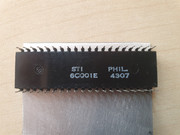
yeh i agree 100% i have to do some work before i can say anything for sure about my module, and the delay required. i have not yet tried that model of ULA.i think the other mark did say that the 7 variant has a CAS delay built in to match the RAS delay that is employed on issue 4A and above (not 4S)dfzx wrote: ↑Mon Oct 30, 2023 8:46 pm The values I chose for those components (68R and 100pF) on my original circuit will produce a CAS delay which should work with any Spectrum with a 6C001E-7 ULA. I've tried it on my 2 Spectrums, one issue 2 and one issue 3, both of which have that ULA, and it works fine on both.
I haven't tested it with other boards, but I know of no reason why it wouldn't work with any board from issue 2 onwards. Admittedly, my knowing no reason isn't saying too much, but I don't think they changed the CAS timings on any of them.I haven't tested it with different ULA versions either. I could believe there might be some subtle differences with ULA versions, but again, I don't know of anything which might cause a problem.
With the exception of issue 1 Spectrums or the very earliest ULA versions, I'd expect my design to work with any combination.
The issue that's popped up here is that mark8bit has redesigned the layout of the board, but as I understand it hasn't yet done the empirical testing of the delay circuit. He's made some significant changes, including removing the internal layers which carry my power and ground planes, and so has changed the characteristics of the board a bit. The ULA appears to be a bit fussy about such things and the delay circuit needs tuning to his new design.
New open lower RAM module design (photoessay)
Re: New open lower RAM module design (photoessay)
Re: New open lower RAM module design (photoessay)
the other thing to consider is that i had the CAS going into the inverter twice after the capacitor/reistor delay so that would also add delay, I'm not sure how much yet till i try and work it out

Re: New open lower RAM module design (photoessay)
If I understand correctly, he also has a problem with wrong resistors on the ZX Spectrum board.dfzx wrote: ↑Mon Oct 30, 2023 8:46 pm The issue that's popped up here is that mark8bit has redesigned the layout of the board, but as I understand it hasn't yet done the empirical testing of the delay circuit. He's made some significant changes, including removing the internal layers which carry my power and ground planes, and so has changed the characteristics of the board a bit. The ULA appears to be a bit fussy about such things and the delay circuit needs tuning to his new design.
I did the math and your extra layers actually represent an extra capacitor of a few pF, so I think this should have negligible impact.
But even if the characteristics of your board were significantly changed by a redesign, there should be an R1 C4 combination that works, right? So one should just try changing the R1 value until it works?
I'd love to join in the testing spree, but I do not have a ZX diagnostic tool. It looks like I could build one following these instructions https://github.com/konkotgit/ZX-external-ROM, and combining the PCBs for the ZX diagnostic tool and the memory module would make the effort more efficient (two PCBs for the price of one). Any thoughts on going down that avenue?
I do not understand this. Comparing the original and your design, all I see is that you fixed A10 instead of A14 at memory chip. The original schematic also used the inverter twice. So there is no change in this regard.
Re: New open lower RAM module design (photoessay)
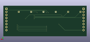
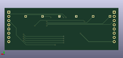
I have recreated mark8bit's two-layer project in KiCAD. The project could be simplified even further if the paths were routed between the pins, but I was afraid that rerouting would change the galvanic properties and cause more problems with signal delays. I only rerouted RAS_INV path as mark8bit's original project used 4 vias, which I think is overkill. Everything else has been replicated as closely as possible:

I also have all the necessary chips, but now I have to wait until mark8bit's design is tested. Ordering the PCB just costs too much (board $2, shipping $7) so it's just too expensive for me to just test it.
I also have all the necessary chips, but now I have to wait until mark8bit's design is tested. Ordering the PCB just costs too much (board $2, shipping $7) so it's just too expensive for me to just test it.
Re: New open lower RAM module design (photoessay)
What price point are you aiming for? You can't optimise away the $7 shipping, so the $2 fabrication cost is the only place to make savings. Re-routing a few tracks and removing a couple of vias isn't going to make any difference to the price.
As I understand things, Mark's re-design has been tested and it's been found that the 2-layer optimisations have stopped the circuit working correctly. It may not be an easy fix.
I've rather lost track of what you're trying to achieve. Do you want a board to put in a broken Spectrum? Or are you simply going through an educational exercise in PCB design optimisation?
Derek Fountain, author of the ZX Spectrum C Programmer's Getting Started Guide and various open source games, hardware and other projects, including an IF1 and ZX Microdrive emulator.
-
1024MAK

- Bugaboo
- Posts: 3123
- Joined: Wed Nov 15, 2017 2:52 pm
- Location: Sunny Somerset in the U.K. in Europe
Re: New open lower RAM module design (photoessay)
In terms of going from a four layer board to a two layer board, the things that may make a significant difference are the width and routing of the 0V/GND and +5V/VCC tracks. These should be as wide as practical, go the most direct route, and both the 0V/GND and +5V/VCC tracks should follow one another as close as possible.
Next up is the control lines. Again, where practical, go the most direct route.
The address and data lines are the lowest in terms of which are the most critical. As the relevant device only samples them under the control of the relevant control line. Hence the voltage on the address and data lines should have time to settle.
Mark
“There are four lights!”
Step up to red alert. Sir, are you absolutely sure? It does mean changing the bulb
Looking forward to summer later in the year.
Re: New open lower RAM module design (photoessay)
The inner layers on my original 4 layer board carried a ground plane and a 5V plane.
Mark's (the other Mark's) re-layout has introduced a ground pour on the top layer, but from what I can tell the tight tracks have stopped the pour from spreading perfectly. The latch, for example, doesn't use the ground pour, it's got a skinny track (with 5 vias) connecting it all the way across to the GND pin. I think the ground impedence has been affected.
+5V is now supplied to the components via tracks. There isn't room for fat ones, but I'd have thought that would be OK. He's still got the decoupling caps in.
TBH I don't know enough about the theory to see where the problem has been introduced. But something appears to have changed in the timing. He's getting the characteristic "sparkles" which indicate the ULA isn't reading the SRAM contents consistently correctly.
Derek Fountain, author of the ZX Spectrum C Programmer's Getting Started Guide and various open source games, hardware and other projects, including an IF1 and ZX Microdrive emulator.
Re: New open lower RAM module design (photoessay)
sorry guys i just keep running out of time.. my prospective is i like to understand everything / educational purposes. or i would have just got a PCB's made up from your project. i have been trying to understand the actual original timing from the original DRAM a bit better complicated by the page mode for ULA reads. i have been reading again "the ULA" book by chris smith.my initial test where that it appears to works fine on a issue 6A,and a issue 3,but had display problem on issue 2 while running roms from external rom boards. one thing i was looking at was removing the CAS from the inverter and just using the delay circuit. thus allowing for a smaller inverter (5 pin i think just for the RAS or even a different register to eliminate the inverter). my PCB routing is a case of learning as i go (i am using easy EDA).. as i recall i was using 10,000mil for signal & 20,000mil for any ground / power that was not included in the plane(but would have to check to be sure).
Re: New open lower RAM module design (photoessay)
The problem as I understand it isn't the ULA as such, it's the SRAM. The RAS/CAS/latching stuff happens which tells the SRAM which byte is required, which it duly fetches and puts on the data bus. It then keeps it there for <some time> which I think is defined as the "hold time." i.e. the amount of time the value is held on the data bus by the SRAM.
The issue appears to be that the SRAM hold time isn't quite long enough, and the SRAM removes the value from the data bus before the ULA has had chance to read it. Or at least, if not "removes it" then it's no longer guaranteed to be there when the ULA reads it. Which in turn means that in many cases the data will still be there and the ULA will correctly read it (maybe outside of the SRAM spec), but just occasionally something else will happen and the data value will be gone when the ULA comes for it.
The PITA is that there's no way (that I found) to be able to tell when the ULA actually reads the byte from the data bus. You can look at your scope traces, and you can try to work out from Chris's book exactly when the ULA came for the byte, but it's hard to be sure the SRAM still had the data on the bus at the moment the ULA came for it.
The correct solution would presumably be add a latch for something which takes the data from the SRAM and holds it for the full time the ULA can ever take, in every machine type, with every ULA type. That would guarantee the data is there when the ULA reads it, even if the SRAM has moved on. But it's complicated.
The option is to add a timing delay to try to get the SRAM and the ULA in perfect sync. But we're talking nanoseconds here, so the goldilocks zone - not to early, not too late - is very, very narrow and easily unsettled by circuit changes.
Derek Fountain, author of the ZX Spectrum C Programmer's Getting Started Guide and various open source games, hardware and other projects, including an IF1 and ZX Microdrive emulator.
Re: New open lower RAM module design (photoessay)
yeh i think the ULA is looking at the data bus 100ns after cas in enabled and the SRAM sends it at about 45ns. i was looking at slower SRAM but they are not so readily available.. i have just been running further tests on the issue 3 is does occasionally get the sparkles but not normally while playing a games or in basic. but briefly when running certain ram checking programs ie zx diagnostic, and also using retroleum smart card on the game loader menu so makes me wonder what they are doing to cause it but game play not. as i would have thought that game play would be stretching the display capabilities the most.
Re: New open lower RAM module design (photoessay)
At JLCPCB, using four layers instead of two layers increases the cost of the PCB by $5. Also, I often combine multiple two-layer PCB designs to reduce costs. Therefore, the four-layer design is impractical for me.dfzx wrote: ↑Fri Nov 10, 2023 8:46 am What price point are you aiming for? You can't optimise away the $7 shipping, so the $2 fabrication cost is the only place to make savings. Re-routing a few tracks and removing a couple of vias isn't going to make any difference to the price.
As I understand things, Mark's re-design has been tested and it's been found that the 2-layer optimisations have stopped the circuit working correctly. It may not be an easy fix.
I've rather lost track of what you're trying to achieve. Do you want a board to put in a broken Spectrum? Or are you simply going through an educational exercise in PCB design optimisation?
Also, following the discussion here, I do not understand what the real advantage of the four-layer design is. Will the DRAM retain the output data longer as a result? I doubt it. My uneducated guess is that a two-layer design should be just as good as any other. The only problem is probably the optimisation of R1/C4 combination in your KiCAD project. If my guess was correct, I would order the PCB immediately and then try different resistors until the timing is right.
My Spectrum is currently working, but freezes occasionally. I suspect that one of the lower DRAMs is unstable, and it is extremely difficult to figure out which one it is under such non-repeatable conditions. So my solution is to build this DRAM module to replace all the lower DRAMs.
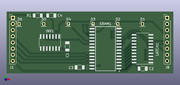
Following your ideas, I further updated my design. Now there are three paths between the ZX ground and the latch ground, one of which is really thick. I have enough room on the bottom to add another direct path if you think it will make a difference. Also, all power paths are as short as possible.dfzx wrote: ↑Fri Nov 10, 2023 11:01 am The inner layers on my original 4 layer board carried a ground plane and a 5V plane.
Mark's (the other Mark's) re-layout has introduced a ground pour on the top layer, but from what I can tell the tight tracks have stopped the pour from spreading perfectly. The latch, for example, doesn't use the ground pour, it's got a skinny track (with 5 vias) connecting it all the way across to the GND pin. I think the ground impedence has been affected.
+5V is now supplied to the components via tracks. There isn't room for fat ones, but I'd have thought that would be OK. He's still got the decoupling caps in.
Also, mark8bit's design had a control line (RAS_INV) with four vias, which I optimised so that it only has two. And I shortened ZX_RAS and ZX_WRITE significantly. KiCAD files are shared here: https://github.com/marko-pi/zx-spectrum-lower-ram
Last edited by Pygmalion on Sat Nov 11, 2023 12:04 am, edited 1 time in total.
-
1024MAK
- Bugaboo
- Posts: 3123
- Joined: Wed Nov 15, 2017 2:52 pm
- Location: Sunny Somerset in the U.K. in Europe
Re: New open lower RAM module design (photoessay)
I’m speculating here, as I’ve not done any investigating.
But modern SRAM is a lot quicker than the SRAM from ten or more years ago. Hence it will switch its outputs off (to high resistance mode) as soon as either the /CE (/CS) or /OE pins goes to the inactive state (which is high).
Whereas older SRAM and DRAM chips take longer to turn off there outputs.
If, and it’s a very big if, this is a problem with the SRAM turning off its outputs before the ULA has latched the data from it. Then the solution is to keep the CE (/CS) and /OE pins in the active state for a short period of time after whichever control signal goes inactive. But it can’t be too long a period of time, otherwise it messes up other things.
The reason why different hardware affects things, is to do with the loading of the data bus.
I don’t know why some software/programs/activity affects it more than others. It shouldn’t. the ULA and the RAM have no idea what each data byte means.
However, there will be a different affect depending on if the Z80 is running machine code from ROM, contended RAM or upper RAM.
Mark
“There are four lights!”
Step up to red alert. Sir, are you absolutely sure? It does mean changing the bulb
Looking forward to summer later in the year.
Re: New open lower RAM module design (photoessay)
As I understand the problem, the main issue here is whether a particular ULA always reads the data at the same time in relation to CAS signal.
If the answer is yes, then the delay circuit of dfzx that delays both the start and the end of the CAS signal is fine, and only the values of Csmall and R2 need to be optimised.
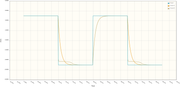
However, if the read timing is different in different situations and for different ULAs, then it might be better to delay only the end of the CAS signal and leave the start of the CAS signal intact. In this case, my naïve suggestion would be to add a fast switching (or perhaps Schottky) diode D7 so that Csmall empties quickly through D7 but charges slowly through R2.
Circuit:
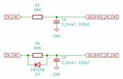
Simulation (orange without diode, gray with diode)
If the answer is yes, then the delay circuit of dfzx that delays both the start and the end of the CAS signal is fine, and only the values of Csmall and R2 need to be optimised.
However, if the read timing is different in different situations and for different ULAs, then it might be better to delay only the end of the CAS signal and leave the start of the CAS signal intact. In this case, my naïve suggestion would be to add a fast switching (or perhaps Schottky) diode D7 so that Csmall empties quickly through D7 but charges slowly through R2.
Circuit:
Simulation (orange without diode, gray with diode)
Last edited by Pygmalion on Sat Nov 11, 2023 10:42 am, edited 1 time in total.
Re: New open lower RAM module design (photoessay)
i will be looking at this again later & your new design . one thing i noticed with the issue 2 was that delaying CAS further did not improve the sparkles but when the CAS got delayed to much they started getting worse.. i was wondering about additional hold for CAS rather than delay as well.
Re: New open lower RAM module design (photoessay)
also most my problems are due to me being pedantic and wanting it to work faultlessly in all situations, in reality i already have a good / satisfactory working solution for most operations of the spectrum. but i will continue.. next is the upper ram module  and the +2 ram module (maybe that could bypass the ZX8401 for the upper 64k) not to mention my switching ROM board module projects etc .. need more hours in the day
Re: New open lower RAM module design (photoessay)
The 4 layer design provides a ground plane and a power plane positioned in the centre layers so they separate the signals on the outer layers. That's best practise for high frequency circuits. The ground plane enables low impedance for returning signals, reduces crosstalk and interference, and reduces noise on the circuit's ground. The +5V plane reduces noise and variation in the power supply. Removing those planes is a commendable optimisation in terms of cost, but it adds complexity and almost certainly reduces signal integrity. I did use them for a reason in the original design. Mark's experimental design has, at least to some extent, confirmed my design choice.
It's nowhere near a certainty that changing the delay timing will fix the problem. It might be that the variations caused by different Spectrum boards, different ULAs and different expansion devices are such that no one timing circuit on the memory board can cater for all scenarios.
My guess is that you're right and it's still a fixable problem. Finding the fix and doing all the testing is clearly a significant task, though.
These are all useful steps forward, but without some very powerful modelling software set up to simulate Spectrums and ULAs and the like, the only way to see if it all helps is to make it, plug it in and see what it does.Pygmalion wrote: ↑Fri Nov 10, 2023 10:48 pm Following your ideas, I further updated my design. Now there are three paths between the ZX ground and the latch ground, one of which is really thick. I have enough room on the bottom to add another direct path if you think it will make a difference. Also, all power paths are as short as possible.
Also, mark8bit's design had a control line (RAS_INV) with four vias, which I optimised so that it only has two. And I shortened ZX_RAS and ZX_WRITE significantly.
Derek Fountain, author of the ZX Spectrum C Programmer's Getting Started Guide and various open source games, hardware and other projects, including an IF1 and ZX Microdrive emulator.
Re: New open lower RAM module design (photoessay)
Yes, that's the gist of it. The SRAM's /OE is permanently on, and /CE is switched by the CAS signal, so in theory when the ULA has read the data and it turns CAS off, the SRAM is fine to remove the value from its output bus and go inactive. In practise that doesn't work. The Z80 is happy, but the ULA's video generation produces flickering corruption "sparkles" all over the screen.
Exactly right. The RC circuit delays CAS by a few tens of nanoseconds. It's therefore a bit slower to turn the SRAM /CE on, which doesn't seem to bother anything, and a bit slower to turn the SRAM /CE off again, hence the value remains in place a bit longer. Then the ULA generates the video correctly and reliably. I appreciate your scepticism, but that's the observation. Tweaking the timing of the CAS signal varies the density of the sparkles, and if you go too far the Z80 stops working.1024MAK wrote: ↑Fri Nov 10, 2023 11:56 pm If, and it’s a very big if, this is a problem with the SRAM turning off its outputs before the ULA has latched the data from it. Then the solution is to keep the CE (/CS) and /OE pins in the active state for a short period of time after whichever control signal goes inactive.
I didn't have a copy of the ULA book when I was looking hard at this. Now I do, but boy does it make the brain hurt...
My "bench Spectrum," which I do all my design work on, is an issue 2 with a 6C001E-7 and one of my memory boards in it. I have a Retroleum Smart Card which occasionally goes into the back, my own Pico-based ROM board and my Microdrive expansion emulator device, both of which I use from time to time, plus other projects I'm tinkering with. I've never seen the sparkles with my hardware and my memory board.
You're right, of course, that the program running on the Z80 is irrelevant to the ULA's video generation, which means the hardware attached to the back of the machine must be changing the behaviour of the memory circuit such that the timings are altered a bit. I'd be very interested to learn why, should the-other-Mark manage to work it out.
Derek Fountain, author of the ZX Spectrum C Programmer's Getting Started Guide and various open source games, hardware and other projects, including an IF1 and ZX Microdrive emulator.
Re: New open lower RAM module design (photoessay)
OK, this is what I wanted to know. I do not understand these fine details as I have no formal training in electrical engineering. I will leave it to the experts among you to come up with a possible solution to the problem.dfzx wrote: ↑Sat Nov 11, 2023 11:44 am The 4 layer design provides a ground plane and a power plane positioned in the centre layers so they separate the signals on the outer layers. That's best practise for high frequency circuits. The ground plane enables low impedance for returning signals, reduces crosstalk and interference, and reduces noise on the circuit's ground. The +5V plane reduces noise and variation in the power supply. Removing those planes is a commendable optimisation in terms of cost, but it adds complexity and almost certainly reduces signal integrity. I did use them for a reason in the original design. Mark's experimental design has, at least to some extent, confirmed my design choice.
But looking at the manuals, I see that with the 4116 the reading is terminated by raising CAS, while with the IS65C256AL-45 the reading is terminated by raising CE/OE. So this should not be a problem. The way I read it, writing should be a problem because the 4116 expects data immediately on lowering CAS and must be available for at least 45ns, while the IS65C256AL-45 expects data only 20ns after lowering WE. [For 4116 WRITE is lowered 40ns before CAS.] Or have I overlooked something again?
To me, this all looks more and more like some kind of magic trick to use undocumented properties of the IS65C256AL-45 chip. Unfortunately, I have already bought the necessary components, so I will just combine my two-layer design with other designs I need and hope for the best. If it does not work, at least I will not have wasted money on the PCB.
By the way, retroleum sells the DRAM replacement again (https://www.retroleum.co.uk/zx-spectrum-chips), but he uses only three chips, so I think he probably uses the same (unreliable) design.
Re: New open lower RAM module design (photoessay)
It's not an unreliable design. It works perfectly well as a 4 layer board.Pygmalion wrote: ↑Sat Nov 11, 2023 1:36 pm By the way, retroleum sells the DRAM replacement again (https://www.retroleum.co.uk/zx-spectrum-chips), but he uses only three chips, so I think he probably uses the same (unreliable) design.
Derek Fountain, author of the ZX Spectrum C Programmer's Getting Started Guide and various open source games, hardware and other projects, including an IF1 and ZX Microdrive emulator.
Re: New open lower RAM module design (photoessay)
i have used retroleum and ZXzigg lower ram modules, and they have always worked perfectly on all issues of spectrum
Re: New open lower RAM module design (photoessay)
So, do Retroleum and ZXzigg ram modules use four layers board?
Re: New open lower RAM module design (photoessay)
The Retroleum board is definitely 4 layer - I have one and have checked. I don't know about the ZX Zigg board, I've never seen one. Judging by that copper pour on the underside, I would guess not.
No one is saying that this memory board can't be made as a 2 layer board. What we know so far is that my original design was 4 layers, and as a 4 layer board it works well. We also know that converting my design to a 2 layer board has not yet been shown to work. That doesn't mean it won't work eventually, and it doesn't mean that 4 layers is the only way to design a lower memory board.
Derek Fountain, author of the ZX Spectrum C Programmer's Getting Started Guide and various open source games, hardware and other projects, including an IF1 and ZX Microdrive emulator.
Re: New open lower RAM module design (photoessay)
OK, thanks for the answer.
As much as I do not understand the difference between two-layer and four-layer design, I would want to understand the timing issue. Has anyone studied the specifications of 4116 DRAM and 32k SRAM? [I have some experience with reading specifications and bitbanging serial and parallel chip communication.]
The first one to come up with this design, as far as I know, is Alwin Hensler. But he did not specify timing details and did not need a delay.
Now you have said that timing is the problem with reading. I do not understand that and I will try to explain why shortly.
In ULA-RAM communication, the ULA is the master and the RAM is the slave, so all control data go exclusively in one direction, from the ULA to the RAM. Therefore, the ULA can control how long the RAM provides data by holding down the CAS/OE/CE line. On the other hand, RAM cannot control how long ULA provides data.
In addition, the waveforms for writing are completely different because the input and output lines are separated in the DRAM, but not in the SRAM. In particular, DRAM expects datum on CAS drop as its input line is always float (ready). On the other hand SRAM expects data some time after WE drop, because it must first put data lines into float (ready), to avoid conflict in communication in both directions.
I could answer some of these questions if I had a good logic analyser. My logic analyser has top frequency of 8 MHz and is good enough for my casual bitbanging, but the RAM communication is much faster and I'd need at least 100 MHz resolution.
Perhaps we can find the cause of the problem more easily if we look into it.
Last edited by Pygmalion on Sun Nov 12, 2023 10:45 am, edited 1 time in total.
Re: New open lower RAM module design (photoessay)
the zxzigg is i believe a 2 layer but using a slower SRAM (55ns) which is not available anymore.
i have been looking at the timing diagrams but i am learning as i go as i do with most things. so what i think is that the CAS delay requirement is more to do with the RAS going through the inverter and delaying it by a few ns and then the CAS goes active before the data is stable on the register lines. as the SRAM appears to hold the data valid as long as the CAS is held low (actually about 20ns after that) and the spectrum would actually hold it LOW for longer as it was required for the DRAM to wait 100ns before accessing the data.
i did some more testing, i made a another board up but bypassed the CAS delay / inverter part completely so the SRAM is seeing the CAS direct from spectrum and this worked in the issue 3 with no sign of problems, but with the issue 2 there is still some sparkles (less in general but more when using the game loader ROM)
Re: New open lower RAM module design (photoessay)
Interesting theory - do you thing inverter and register would need more than 20ns to do their stuff? RAS to CAS delay time is 20 ns.mark8bit wrote: ↑Sun Nov 12, 2023 10:42 am i have been looking at the timing diagrams but i am learning as i go as i do with most things. so what i think is that the CAS delay requirement is more to do with the RAS going through the inverter and delaying it by a few ns and then the CAS goes active before the data is stable on the register lines. as the SRAM appears to hold the data valid as long as the CAS is held low (actually about 20ns after that) and the spectrum would actually hold it LOW for longer as it was required for the DRAM to wait 100ns before accessing the data.
As for the rest, both SRAM and DRAM hold data minimum 0ns after releasing CAS/OE/CE lines (20ns is maximum for DRAM!), so I believe ULA is reading data before releasing CAS/OE/CE. And before releasing CAS/OE/CE, both SRAM and DRAM must keep the data available. I simply don't see problem here.
Can you tell if those sparkles are read or write problem? If they were read problem I'd expect sparkles move, while if they were write problem, I'd expect sparkles being fixed.mark8bit wrote: ↑Sun Nov 12, 2023 10:42 am i did some more testing, i made a another board up but bypassed the CAS delay / inverter part completely so the SRAM is seeing the CAS direct from spectrum and this worked in the issue 3 with no sign of problems, but with the issue 2 there is still some sparkles (less in general but more when using the game loader ROM)