
I also discovered this project and, while tinkering with the original KiCAD project, came to the conclusion that it could be simplified considerably: Reduce to two levels, reduce the number of vias, etc. I am glad that others have come to the same conclusion!
Also, is it absolutely necessary to use a separate capacitor for each chip?
How come the older project https://web.archive.org/web/20090728053 ... placement/ does not need a CAS delay circuit?
Since some have already simplified the PCB, I wonder if it is possible to share the result so that I do not have to waste my time simplifying it again?
New open lower RAM module design (photoessay)
Re: New open lower RAM module design (photoessay)
the link is from a different project, i think Derek did his from scratch, the need for CAS delay i think is the access speed of the Sram used, i suspect the other caps could be removed, i may try this tomorrow. with mine i mixed all the data / address lines up in order to make the shortest routes i want to try it on a +2 as well depending on if i can source some 64k Sram at a decent price. i did put one of mine on a 16k issue 2 and there is screen corruption, but i am hopping this is a different fault so more testing needed before i can say for sure. i do plan on making any of my projects available to anybody that is interested.
Re: New open lower RAM module design (photoessay)
As Mark says, I did my design from scratch. I didn't know about Alwin's design, buried in the Internet Archive from 2009.Pygmalion wrote: ↑Sat Oct 14, 2023 10:39 pm I also discovered this project and, while tinkering with the original KiCAD project, came to the conclusion that it could be simplified considerably: Reduce to two levels, reduce the number of vias, etc. I am glad that others have come to the same conclusion!
My starting point was knowing little about electronics, so I had to learn an awful lot, and it took a huge effort to get it working. I'm aware it's not the optimum design, but I made it open and available to anyone who wants to improve it.
From what I've seen, the 5V power supply inside the Spectrum is pretty stable, so you might get away with reduced decoupling, but as soon as you start adding devices on the back, or using replacement keyboards and the like, that is likely to change. This is memory, so one little sag on the supply represents a possible crash which would be impossible to debug or reproduce.
Mark's right again, it's due to the timing on the SRAM I used. Specifically the data hold time if I recall correctly. If you can source an SRAM which has a hold time more compatible with the ULA (which means all variants of the ULA) you can do away with the RC delay. Alwin's Toshiba chip appears to be obsolete, but new old stock is available on eBay if you want to spend £15 a pop or risk a Chinese knockoff.Pygmalion wrote: ↑Sat Oct 14, 2023 10:39 pm How come the older project https://web.archive.org/web/20090728053 ... placement/ does not need a CAS delay circuit?
Derek Fountain, author of the ZX Spectrum C Programmer's Getting Started Guide and various open source games, hardware and other projects, including an IF1 and ZX Microdrive emulator.
Re: New open lower RAM module design (photoessay)
Thank you for your reply.dfzx wrote: ↑Sun Oct 15, 2023 11:18 am From what I've seen, the 5V power supply inside the Spectrum is pretty stable, so you might get away with reduced decoupling, but as soon as you start adding devices on the back, or using replacement keyboards and the like, that is likely to change. This is memory, so one little sag on the supply represents a possible crash which would be impossible to debug or reproduce.
Mark's right again, it's due to the timing on the SRAM I used. Specifically the data hold time if I recall correctly. If you can source an SRAM which has a hold time more compatible with the ULA (which means all variants of the ULA) you can do away with the RC delay. Alwin's Toshiba chip appears to be obsolete, but new old stock is available on eBay if you want to spend £15 a pop or risk a Chinese knockoff.
If I understand you correctly, a simplified design with two layers should also suffice. There is no particular reason why you included these two extra layers. And your delay circuit is simply the consequence that a different SRAM was used. Can you confirm these two things?
As for the capacitors, I understand the reason, but I think one larger capacitor should be enough for all three chips. After all, the copper paths are not that long to make a difference.
Re: New open lower RAM module design (photoessay)
Thank you very much for your reply. I will be happy to use your design when it is finally tested.mark8bit wrote: ↑Sat Oct 14, 2023 11:50 pm the link is from a different project, i think Derek did his from scratch, the need for CAS delay i think is the access speed of the Sram used, i suspect the other caps could be removed, i may try this tomorrow. with mine i mixed all the data / address lines up in order to make the shortest routes i want to try it on a +2 as well depending on if i can source some 64k Sram at a decent price. i did put one of mine on a 16k issue 2 and there is screen corruption, but i am hopping this is a different fault so more testing needed before i can say for sure. i do plan on making any of my projects available to anybody that is interested.
I am not in a hurry. I always collect a few PCB projects and make a composite PCB before sending it to JLCPCB. Ordering for just one PCB ($2 + $6 shipping) is not very cost effective.
Re: New open lower RAM module design (photoessay)
Yes, confirmed.Pygmalion wrote: ↑Sun Oct 15, 2023 12:33 pm If I understand you correctly, a simplified design with two layers should also suffice. There is no particular reason why you included these two extra layers. And your delay circuit is simply the consequence that a different SRAM was used. Can you confirm these two things?
Derek Fountain, author of the ZX Spectrum C Programmer's Getting Started Guide and various open source games, hardware and other projects, including an IF1 and ZX Microdrive emulator.
Re: New open lower RAM module design (photoessay)
yeh i use JLPCB and its always the postage to the UK that hits the hardest, although there pricing is strange there per unit price tends to be cheaper for less quantity.. i always go for the absolute cheapest postage and it has always arrived (eventually) .
and the PCB's have always been really good never had a problem..
i just seems crazy that we have to buy from another country.. i'm looking at git hub and git (to share my projects) something i have no knowledge of but YouTube is coming to the rescue
and the PCB's have always been really good never had a problem..
i just seems crazy that we have to buy from another country.. i'm looking at git hub and git (to share my projects) something i have no knowledge of but YouTube is coming to the rescue
-
1024MAK

- Bugaboo
- Posts: 3123
- Joined: Wed Nov 15, 2017 2:52 pm
- Location: Sunny Somerset in the U.K. in Europe
Re: New open lower RAM module design (photoessay)
No. But, having plenty of capacitors to provide enough decoupling to prevent strange hard to trace problems is a must. As they are cheap, and semiconductor manufacturers recommend one decoupling capacitor per chip (mounted as close as possible to the chips supply and ground pins), it’s now normal standard practice to have one per chip.
Timing.Pygmalion wrote: ↑Sat Oct 14, 2023 10:39 pm How come the older project https://web.archive.org/web/20090728053 ... placement/ does not need a CAS delay circuit?
Firstly, the original ZX Spectrum design and the ULAs were discovered to not provide the correct timing for the 4116 DRAM chips. Although most DRAM did actually work. Having discovered this, part way through the life of the ZX Spectrum, Sinclair changed the design slightly to correct this problem. Hence different issue boards and different ULA chip versions have slightly different timing.
Secondly, modern SRAM chips are far faster than the older SRAM chips. Because of this, some need one of control signals to be delayed slightly. This problem also occurs when upgrading a ZX81 with modern SRAM chips.
It’s possible that Alwin did not encounter any problems with his design at the time.
Mark
“There are four lights!”
Step up to red alert. Sir, are you absolutely sure? It does mean changing the bulb
Looking forward to summer later in the year.
-
1024MAK
- Bugaboo
- Posts: 3123
- Joined: Wed Nov 15, 2017 2:52 pm
- Location: Sunny Somerset in the U.K. in Europe
Re: New open lower RAM module design (photoessay)
No, one larger capacitor is not the same. The whole point of having a capacitor to decouple the supply to a chip is to minimise the voltage change at the pins of the chip. The PCB tracks have a small amount of inductance and resistance. It may not be much, but if the chip is switching it’s outputs at a very fast rate, this small amount of inductance and resistance is significant.
For example, the LYONTEK LY62256PL-55LLI 32k byte SRAM chip has an access time of only 55ns, so the outputs will be changing state at a far faster rate. That’ puts it in the megahertz range of frequencies. And the chip needs enough power to operate its internal circuitry and drive eight datalines simultaneously, including charging up the stray capacitance of the ZX Spectrum’s databus.
Mark
“There are four lights!”
Step up to red alert. Sir, are you absolutely sure? It does mean changing the bulb
Looking forward to summer later in the year.
Re: New open lower RAM module design (photoessay)
The problem with the cheapest shipping is that it would almost certainly end up in my country's customs office. And my country's post office charges about $3 just to deal with the customs office. So I would probably save as much as I paid later.
Re: New open lower RAM module design (photoessay)
One decoupling capacitor might be enough if you have 4 layer pcb with solid ground and power planes. But it's better to have them anyway. It's no fun trying to fix power supply issues.
Capacitors cheap small and easy to solder.
Capacitors cheap small and easy to solder.
Re: New open lower RAM module design (photoessay)
I have repaired my ZX Spectrum by replacing the DRAM chips with those obtained at AliExpress. 
I am therefore interested in making low memory adapter for future use. Please, if you can, share files for the board optimised for two layers as soon as it is tested. Thanks.
I am therefore interested in making low memory adapter for future use. Please, if you can, share files for the board optimised for two layers as soon as it is tested. Thanks.
Re: New open lower RAM module design (photoessay)
i am no further forward with the testing.
but i have spent the time to learn how to post my project on github so have put it there.
https://github.com/marksummerton/zx-spe ... module.git
but i have spent the time to learn how to post my project on github so have put it there.
https://github.com/marksummerton/zx-spe ... module.git
Re: New open lower RAM module design (photoessay)
Great!mark8bit wrote: ↑Sun Oct 29, 2023 12:01 pm i am no further forward with the testing.
but i have spent the time to learn how to post my project on github so have put it there.
https://github.com/marksummerton/zx-spe ... module.git
Have you tried putting it in your ZX Spectrum to see if it works?
As far as I can tell, the positioning of chips is optimal.
Since I will be combining several PCBs into one order (JLCPCB allows that), I would also need KiCAD files. But even if you do not provide them, I can use your design to create my own KiCAD project.
Re: New open lower RAM module design (photoessay)
have tried in a issue 6A which seemed fine, have also put one in a issue 2 that worked and passed tests, but there was some screen corruption but i'm not sure if that is another fault with the machine (maybe cpu or ic3/ic4 ..keep meaning to do some more testing on that machine, but always seem to run out of time and looking at other projects and 3d printing stuff..
i included the gerber files for the board in the rev 1+3 folders. which can be used to get boards from JLPCB. i don't use KICAD (yet)
i included the gerber files for the board in the rev 1+3 folders. which can be used to get boards from JLPCB. i don't use KICAD (yet)
Re: New open lower RAM module design (photoessay)
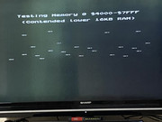
This is currently what I get on the issue 2 .. (only a 16k) seems only when edge connector running though so I need to look at that closer ie just put smart card in on game loading menu and it was doing it but when I load jetpac from it, it works perfectly except I kept crashing into monsters
Re: New open lower RAM module design (photoessay)
That's what I referred to as "sparkles" in the very first post of this thread. Your CAS delay timing is slightly off. The Z80, which is the more tolerant device, is happy and working, but the ULA, which is a lot more fussy, is just occasionally getting a corrupted byte from the SRAM when it's building the screen image.
I've tried my original board in my issue 2 and issue 3 machines, and it works correctly in those. But I learned in another thread a day or two back that the issue 4 boards had some timing changes to the lower memory circuit, which made me wonder if my design would work on those. But those changes seem to be RAS-related, not CAS, so it's probably OK.
Anyway, you're going to need to do some very careful timing with your 'scope to work out exactly what's out of sync. Do you know what ULA is in your issue 2?
Derek Fountain, author of the ZX Spectrum C Programmer's Getting Started Guide and various open source games, hardware and other projects, including an IF1 and ZX Microdrive emulator.
-
1024MAK
- Bugaboo
- Posts: 3123
- Joined: Wed Nov 15, 2017 2:52 pm
- Location: Sunny Somerset in the U.K. in Europe
Re: New open lower RAM module design (photoessay)
That post on DRAM timing is here.
In an issue one or issue two, the multiplexer control signal is taken straight from the /RAS signal from the ULA. This was changed on issue 4A and subsequent boards (see the link above).
Because the multiplexer control signal was changed, they (Sinclair) also had to change the /CAS timing. This alteration was done in the ULA chip.
Mark
“There are four lights!”
Step up to red alert. Sir, are you absolutely sure? It does mean changing the bulb
Looking forward to summer later in the year.
Re: New open lower RAM module design (photoessay)
cool, more work required then, shame i soldered the module to the motherboard on the issue 2. the 'sparkles' are more rhythmic than random as well.
the issue 2 has a 6C001E-7 but the resistors where set up for the earlier ULA 5C112E (R49,R47,R56,R63) so first thing i tried was updating those, there is also a branch off RAS going to cpu refresh via R56 but this resistor is not fitted (think this was leftover from issue 1 ?) . i did try to get the issue 6A to show the 'sparkles' by changing the cap/resistor time delay but it was resistant. i am going to check the 6A board again but if i am reading the schematic correct it sends both CAS & RAS into IC28 for a double hit to delay both before going into ZX8401 (essentially IC3,IC4 without any additional delay .seems that IC28 should have been incorporated into ZX8401. although the 4A does not appear to have this additional delay on CAS only the RAS..
the issue 2 has a 6C001E-7 but the resistors where set up for the earlier ULA 5C112E (R49,R47,R56,R63) so first thing i tried was updating those, there is also a branch off RAS going to cpu refresh via R56 but this resistor is not fitted (think this was leftover from issue 1 ?) . i did try to get the issue 6A to show the 'sparkles' by changing the cap/resistor time delay but it was resistant. i am going to check the 6A board again but if i am reading the schematic correct it sends both CAS & RAS into IC28 for a double hit to delay both before going into ZX8401 (essentially IC3,IC4 without any additional delay .seems that IC28 should have been incorporated into ZX8401. although the 4A does not appear to have this additional delay on CAS only the RAS..
Re: New open lower RAM module design (photoessay)
* i misunderstood the schematic CAS is not further delayed at all..
-
1024MAK
- Bugaboo
- Posts: 3123
- Joined: Wed Nov 15, 2017 2:52 pm
- Location: Sunny Somerset in the U.K. in Europe
Re: New open lower RAM module design (photoessay)
Resistors R47, R49, R56 and R63 are part of the analogue video system so are nothing to do with the DRAM timing.
The branch to /RAS via R57 is redundant as this has never worked, hence Sinclair did not fit R57 and removed the associated PCB tracks in later issue boards. It was supposed to allow the Z80A to provide DRAM refresh during the time the ULA is not ‘drawing the screen’ but the system works fine without it.
On the issue 6A, the /RAS from the ULA (pin 35) goes to a link selection. Normally it then goes to IC28 (74LS04 pin 11), wired as two inverters. The output (pin 12) goes back to the link selection, then normally on to IC27 (ZX8401 pin 1).
See a photo of an issue 6A here. The link selection is right next to IC28 right in the centre of the board.
/CAS is delayed in the ULA.
Mark
“There are four lights!”
Step up to red alert. Sir, are you absolutely sure? It does mean changing the bulb
Looking forward to summer later in the year.
Re: New open lower RAM module design (photoessay)
ohh yeh the schematic makes sense now. hade a marathon ram checking session..
removed the lower ram in a non working issue 3 board, and the module worked perfect although seems to be fine with or without the CAS delay from the resistor/capacitor the same as the issue 6A. tried varying the CAS time time delay on the issue 2 with little or no change, although it was less so without the 3 filter capacitors fitted (100nf) and i found that if i touched the left hand row of pins on the module (dram pins 1 - 8) then i could make the 'sparkles' disappear completely !!!
removed the lower ram in a non working issue 3 board, and the module worked perfect although seems to be fine with or without the CAS delay from the resistor/capacitor the same as the issue 6A. tried varying the CAS time time delay on the issue 2 with little or no change, although it was less so without the 3 filter capacitors fitted (100nf) and i found that if i touched the left hand row of pins on the module (dram pins 1 - 8) then i could make the 'sparkles' disappear completely !!!
Re: New open lower RAM module design (photoessay)
We're talking small numbers of nano-seconds here, so a bit of extra capacitance here or there can make a notable difference. I found when developing the board that letting the Spectrum warm up for 20 minutes also made the sparkles go away.
Derek Fountain, author of the ZX Spectrum C Programmer's Getting Started Guide and various open source games, hardware and other projects, including an IF1 and ZX Microdrive emulator.
Re: New open lower RAM module design (photoessay)
As far as I understand, the delay depends on the values of the capacitor C4 and the resistor R1. Does this mean that these two values have to be adjusted for each different ZX Spectrum or rather each different ULA chip?
My ULA is 6C001E.
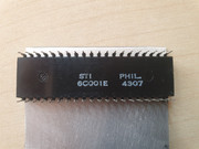
My ULA is 6C001E.
Re: New open lower RAM module design (photoessay)
The values I chose for those components (68R and 100pF) on my original circuit will produce a CAS delay which should work with any Spectrum with a 6C001E-7 ULA. I've tried it on my 2 Spectrums, one issue 2 and one issue 3, both of which have that ULA, and it works fine on both.
I haven't tested it with other boards, but I know of no reason why it wouldn't work with any board from issue 2 onwards. Admittedly, my knowing no reason isn't saying too much, but I don't think they changed the CAS timings on any of them.
With the exception of issue 1 Spectrums or the very earliest ULA versions, I'd expect my design to work with any combination.
The issue that's popped up here is that mark8bit has redesigned the layout of the board, but as I understand it hasn't yet done the empirical testing of the delay circuit. He's made some significant changes, including removing the internal layers which carry my power and ground planes, and so has changed the characteristics of the board a bit. The ULA appears to be a bit fussy about such things and the delay circuit needs tuning to his new design.
Derek Fountain, author of the ZX Spectrum C Programmer's Getting Started Guide and various open source games, hardware and other projects, including an IF1 and ZX Microdrive emulator.